- 您现在的位置:买卖IC网 > Sheet目录1998 > ICS87946AYILFT (IDT, Integrated Device Technology Inc)IC CLOCK GENERATOR 32-LQFP
ICS87946AYI REVISION B JUNE 22, 2012
7
2012 Integrated Device Technology, Inc.
ICS87946I Data Sheet
LOW SKEW, ÷1, ÷2 LVCMOS/LVTTL CLOCK GENERATOR
Application Information
Recommendations for Unused Input and Output Pins
Inputs:
CLK Inputs
For applications not requiring the use of a clock input, it can be left
floating. Though not required, but for additional protection, a 1k
resistor can be tied from the CLK input to ground.
LVCMOS Control Inputs
All control pins have internal pullups or pulldowns; additional
resistance is not required but can be added for additional protection.
A 1k
resistor can be used.
Outputs:
LVCMOS Outputs
All unused LVCMOS output can be left floating. There should be no
trace attached.
Reliability Information
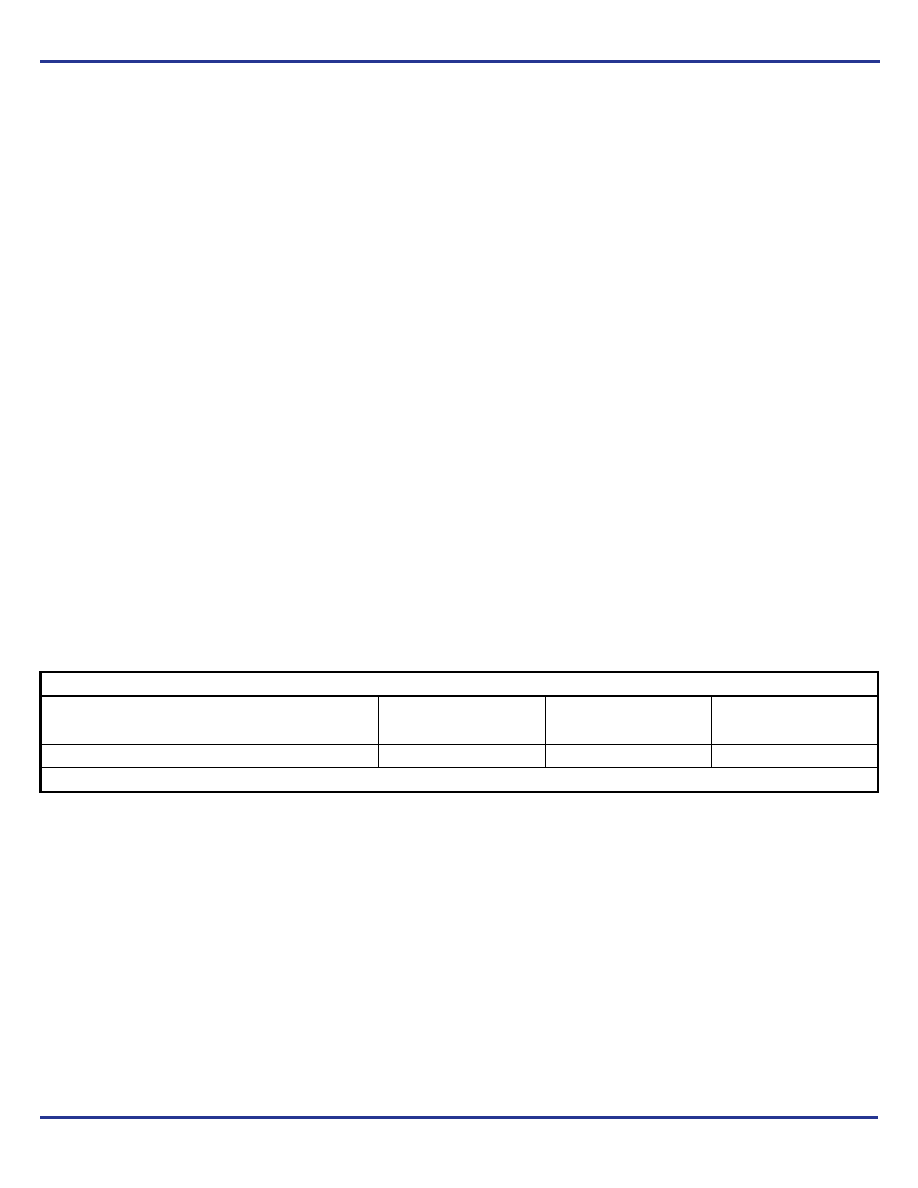
Table 6. θJA vs. Air Flow Table
Transistor Count
The transistor count for ICS87946I is: 1204
θ
JA vs. Air Flow (Linear Feet per Minute)
Linear Feet per Minute
0200
500
Single-Layer PCB, JEDEC Standard Test Boards
67.8°C/W
55.9°C/W
50.1°C/W
Multi-Layer PCB, JEDEC Standard Test Boards
47.9°C/W
42.1°C/W
39.4°C/W
NOTE: Most modern PCB designs use multi-layered boards. The data in the second row pertains to most designs.
发布紧急采购,3分钟左右您将得到回复。
相关PDF资料
ICS87949AYILFT
IC CLOCK GEN LVCMOS 52-LQFP
ICS87950BYILF
IC CLK MULT LVCMOS/LVTTL 32-LQFP
ICS87952AYI-147LF
IC CLK MULT/ZD BUFFER 32-LQFP
ICS87972DYI-147LF
IC CLK MULT/ZD BUFFER 52-LQFP
ICS87973DYI-147LF
IC CLK MULT/ZD BUFFER 52TQFP
ICS87973DYILFT
IC CLK MULT/ZD BUFFER 52-LQFP
ICS87974CYILF
IC CLK GEN LVCMOS/LVTTL 52-LQFP
ICS894D115AGI-04LF
IC CLK/DATA RECOVERY 20-TSSOP
相关代理商/技术参数
ICS87949AYI
制造商:ICS 功能描述:
ICS87949AYILF
功能描述:IC CLK GENERATOR /1 /2 52-LQFP RoHS:是 类别:集成电路 (IC) >> 时钟/计时 - 时钟发生器,PLL,频率合成器 系列:HiPerClockS™ 标准包装:2,000 系列:- 类型:PLL 频率合成器 PLL:是 输入:晶体 输出:时钟 电路数:1 比率 - 输入:输出:1:1 差分 - 输入:输出:无/无 频率 - 最大:1GHz 除法器/乘法器:是/无 电源电压:4.5 V ~ 5.5 V 工作温度:-20°C ~ 85°C 安装类型:表面贴装 封装/外壳:16-LSSOP(0.175",4.40mm 宽) 供应商设备封装:16-SSOP 包装:带卷 (TR) 其它名称:NJW1504V-TE1-NDNJW1504V-TE1TR
ICS87949AYILFT
功能描述:IC CLOCK GEN LVCMOS 52-LQFP RoHS:是 类别:集成电路 (IC) >> 时钟/计时 - 时钟发生器,PLL,频率合成器 系列:HiPerClockS™ 标准包装:1,000 系列:- 类型:时钟/频率合成器,扇出分配 PLL:- 输入:- 输出:- 电路数:- 比率 - 输入:输出:- 差分 - 输入:输出:- 频率 - 最大:- 除法器/乘法器:- 电源电压:- 工作温度:- 安装类型:表面贴装 封装/外壳:56-VFQFN 裸露焊盘 供应商设备封装:56-VFQFP-EP(8x8) 包装:带卷 (TR) 其它名称:844S012AKI-01LFT
ICS87950BYILF
功能描述:IC CLK MULT LVCMOS/LVTTL 32-LQFP RoHS:是 类别:集成电路 (IC) >> 时钟/计时 - 时钟发生器,PLL,频率合成器 系列:HiPerClockS™ 标准包装:1,000 系列:- 类型:时钟/频率合成器,扇出分配 PLL:- 输入:- 输出:- 电路数:- 比率 - 输入:输出:- 差分 - 输入:输出:- 频率 - 最大:- 除法器/乘法器:- 电源电压:- 工作温度:- 安装类型:表面贴装 封装/外壳:56-VFQFN 裸露焊盘 供应商设备封装:56-VFQFP-EP(8x8) 包装:带卷 (TR) 其它名称:844S012AKI-01LFT
ICS87950BYILFT
功能描述:IC CLOCK MULT 1-9 32-LQFP RoHS:是 类别:集成电路 (IC) >> 时钟/计时 - 时钟发生器,PLL,频率合成器 系列:HiPerClockS™ 标准包装:1,000 系列:- 类型:时钟/频率合成器,扇出分配 PLL:- 输入:- 输出:- 电路数:- 比率 - 输入:输出:- 差分 - 输入:输出:- 频率 - 最大:- 除法器/乘法器:- 电源电压:- 工作温度:- 安装类型:表面贴装 封装/外壳:56-VFQFN 裸露焊盘 供应商设备封装:56-VFQFP-EP(8x8) 包装:带卷 (TR) 其它名称:844S012AKI-01LFT
ICS87951AYI-147LF
功能描述:IC BUFFER ZD 1-9 LOW SKEW 32LQFP RoHS:是 类别:集成电路 (IC) >> 时钟/计时 - 时钟发生器,PLL,频率合成器 系列:HiPerClockS™ 标准包装:1,000 系列:- 类型:时钟/频率合成器,扇出分配 PLL:- 输入:- 输出:- 电路数:- 比率 - 输入:输出:- 差分 - 输入:输出:- 频率 - 最大:- 除法器/乘法器:- 电源电压:- 工作温度:- 安装类型:表面贴装 封装/外壳:56-VFQFN 裸露焊盘 供应商设备封装:56-VFQFP-EP(8x8) 包装:带卷 (TR) 其它名称:844S012AKI-01LFT
ICS87951AYI-147LFT
功能描述:IC BUFFER ZD 1-9 LOW SKEW 32LQFP RoHS:是 类别:集成电路 (IC) >> 时钟/计时 - 时钟发生器,PLL,频率合成器 系列:HiPerClockS™ 标准包装:1,000 系列:- 类型:时钟/频率合成器,扇出分配 PLL:- 输入:- 输出:- 电路数:- 比率 - 输入:输出:- 差分 - 输入:输出:- 频率 - 最大:- 除法器/乘法器:- 电源电压:- 工作温度:- 安装类型:表面贴装 封装/外壳:56-VFQFN 裸露焊盘 供应商设备封装:56-VFQFP-EP(8x8) 包装:带卷 (TR) 其它名称:844S012AKI-01LFT
ICS87951AYILF
功能描述:IC CLK ZDB 1:9 180MHZ 32LQFP RoHS:是 类别:集成电路 (IC) >> 时钟/计时 - 时钟发生器,PLL,频率合成器 系列:HiPerClockS™ 标准包装:2,000 系列:- 类型:PLL 频率合成器 PLL:是 输入:晶体 输出:时钟 电路数:1 比率 - 输入:输出:1:1 差分 - 输入:输出:无/无 频率 - 最大:1GHz 除法器/乘法器:是/无 电源电压:4.5 V ~ 5.5 V 工作温度:-20°C ~ 85°C 安装类型:表面贴装 封装/外壳:16-LSSOP(0.175",4.40mm 宽) 供应商设备封装:16-SSOP 包装:带卷 (TR) 其它名称:NJW1504V-TE1-NDNJW1504V-TE1TR